SFP56 Testing Board Design Note
I will record the note of design a SFP56 Testing board.
There are multiple types of SFP connectors:
- SFP 20 pin connector supporting a variety of speeds
- SFP+ Same as SFP but supporting up to 16 Gbps
- SFP28 Also 20 pins, but in an alternative form factor and supporting higher data rates
- SFP56 Same as SFP28 but with higher speed limit
SFP56 Connector Pin
While we using a connector, one of the trouble thing is to find the right pin define. Some time it will confuse and very easy to make mistake. We'd better to check the pin define with a sample of SFP connector before we start designing the board .
Here is the pin define of SFP56 connector:
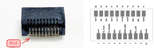
SFP pin number, view from front
| Pin | Symbol | Name/Description | Notes |
|---|---|---|---|
| 1 | VEET | Transmitter Ground (Common with Receiver Ground) | 1 |
| 2 | TFAULT | Transmitter Fault. | 2,3 |
| 3 | TDIS | Transmitter Disable. Laser output disabled on high or open. | 4 |
| 4 | SDA | 2 - wire Serial Interface Data Line | 2 |
| 5 | SCL | 2 - wire Serial Interface Clock Line | 2 |
| 6 | MOD_ABS | Module Absent. Grounded within the module | 5 |
| 7 | RS0 | Rate Select 0. | 5 |
| 8 | RX_LOS | Loss of Signal indication. Logic 0 indicates normal operation. | 6 |
| 9 | RS1 | Rate Select 1. | 5 |
| 10 | VEER | Receiver Ground (Common with Transmitter Ground) | 1 |
| 11 | VEER | Receiver Ground (Common with Transmitter Ground) | 1 |
| 12 | RD - | Receiver Inverted DATA out. AC Coupled | |
| 13 | RD + | Receiver Non - inverted DATA out. AC Coupled | |
| 14 | VEER | Receiver Ground (Common with Transmitter Ground) | 1 |
| 15 | VCCR | Receiver Power Supply | 7 |
| 16 | VCCT | Transmitter Power Supply | 7 |
| 17 | VEET | Transmitter Ground (Common with Receiver Ground) | 1 |
| 18 | TD + | Transmitter Non - Inverted DATA in. AC Coupled. | |
| 19 | TD - | Transmitter Inverted DATA in. AC Coupled. | |
| 20 | VEET | Transmitter Ground (Common with Receiver Ground) | 1 |
Notes:
- Circuit ground is internally isolated from chassis ground.
- Open collector/drain output, which should be pulled up with a 4.7k to 10k Ohm resistor on the host board if intended for use. Pull up voltage should be between 2.0V to Vcc + 0.3V.
- A high output indicates a transmitter fault caused by either the TX bias current or the TX output power exceeding the preset alarm thresholds. A low output indicates normal operation. In the low state, the output is pulled to <0.8V.
- Laser output disabled on TDIS >2.0V or open, enabled on TDIS <0.8V.
- Internally pulled down per SFF-8431 Rev 4.1.
- LOS is open collector output. Should be pulled up with 4.7k to 10kΩ on host board to a voltage between 2.0V and Vcc + 0.3V. Logic 0 indicates normal operation; logic 1 indicates loss of signal.
- Internally connected.
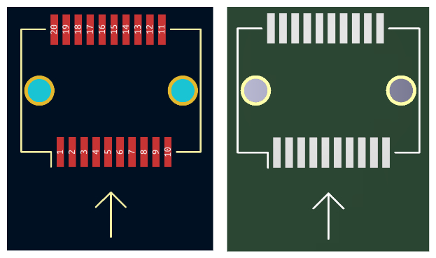
SFP Connector Footprint
We need solder the SFP connector to the board. So it also need to know the footprint of SFP connector. This image direction is same as the above connector picture. The pin 1 is on the left bottom corner. And there are two holes on the PCB for connector alignment.
Layout Consideration
Some suggestion from Zachariah Peterson
- On the right side of the connector, there are I2C interface and some control signals. All of these are low speed and should generally be routed away from the high-speed differential pairs coming to the left side.
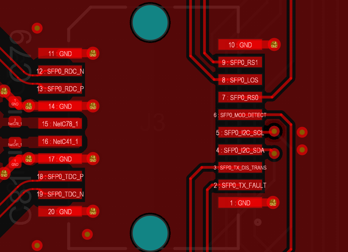
- the high-speed signals enter from the left side, and they are surrounded by GND and PWR pins. The Rx and Tx input/output differential pairs on L1 are marked with yellow arrows:
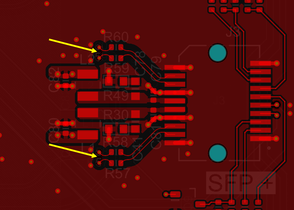
- These lines are passing into the inner layers using differential vias, the vias drop down to L6 in an 8-layer PCB. Because the outer two dielectrics are thin (11 mil total thickness), the stub length is already minimized on this via transition and backdrilling is not needed. The differential pairs pass through an optimized antipad that sets the required differential impedance to 100 Ohms up to a bandwidth of approximately 10 GHz.
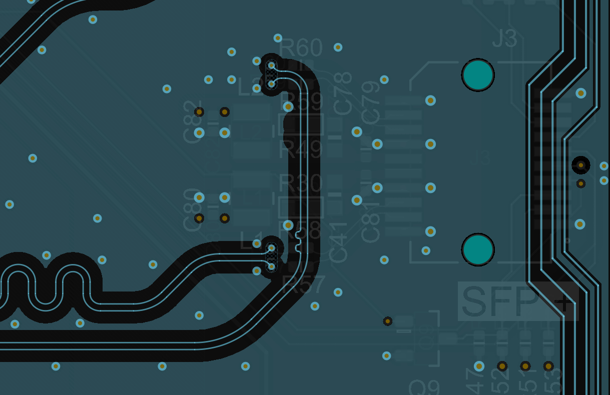
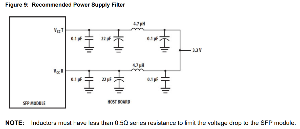
- Power Integrity
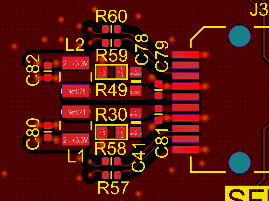
Filter circuit used on the 3V3 rail for powering the transceiver module.
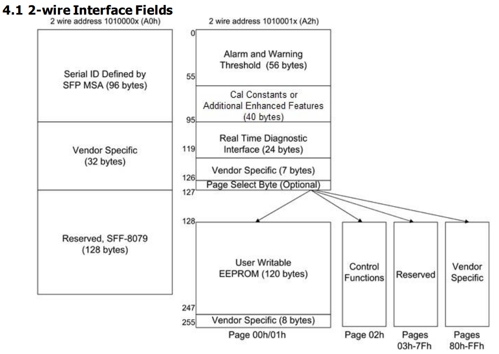
SFP Memory Define
SFF-8472 defines the digital interface of SFP module.
- The interface is accessed via the I2C interface.
- It using two 8-bit addresses: 1010000X (A0h) and 1010001X (A2h),.
A general overview of the memory map is shown below:
Share this article
Comments
0Please sign in to post a comment.
No comments yet.